
The Evolution of PCB Sizing
The advent of printed circuit boards was considered to be a major leap forward in electronic technology when they were first produced in the 1950s. Compared to the previously used point-to-point construction techniques, the introduction of PCBs allowed for electronics to work more safely and efficiently. They were also much more compact and easier to mass produce.
It is this emphasis on compactness that we will focus on in this blog. As technology has evolved PCBs have needed to change too. Most significantly, they have had to keep up with the size demands of modern technology. The public are attracted to increasingly compact electronics. So how have PCBs managed to adapt to these demands, and how will they continue to miniaturise in the future?

From through-hole to surface mount technology (SMT)
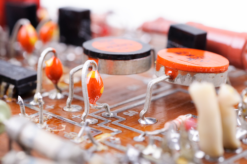
On the original PCBs, components were attached to the board using through-hole technology (pictured above). Small holes were drilled into the board for the components to be slotted into. Wires connected these components. This was laborious, as component leads needed to be formed prior to insertion, and the holes had to be perfectly positioned for each component. There was much more scope for manufacture error.
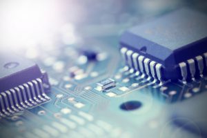
Engineers reasoned that the through-hole mounting technique could be improved upon. Instead, components could be soldered to metal pads on the board – or ‘surface mounted’.
Through-hole technology had been restrictive in regards to component placement. Surface mount technology meant that components could be attached on both sides. This of course allowed for PCBs to be a lot smaller. The components themselves can also be smaller on SMT devices, minimising the overall size even more. In fact, SMT printed circuit boards can be one-quarter to one-tenth the size and weight of their through-hole counterparts. SMT devices can be fitted by a machine and require much less manual intervention.
At Newbury Electronics we make prolific use of surface mount technology. Our placement machines can handle the installation of almost all SMT components. Our proficiency in the use of this technology has been appreciated and employed by companies such as Soundbeam. The Soundbeam is a device which allows the user to make music through movement. They required their PCBs to be very compact and thin. Our advanced surface mount knowledge meant that we were able to rise to the challenge.
Component miniaturisation
As PCB components have gotten smaller, naturally the overall size of PCBs have followed. Circuits used to be made from separate transistors. Custom chips are now more commonly used, which allow the transistors to be far smaller. More transistors can now be packed into less space, leading to faster PCBs that are also more compact. Other components such as resistors have also massively shrunk.
PCB Train used compact PCB technology in their work with Satellite Applications Catapult. The size and weight of satellites meant that they were very expensive to launch. Satellite Applications Catapult wanted to reduce the size and weight of satellites so that multiple launches were possible – thus reducing the cost. They wanted the end product to be as small as possible. PCB Train provided PCBs that were slightly smaller than a credit card to meet the size demands of the compact satellite.
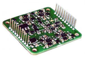
Multi layering
As PCBs have become capable of featuring more and more layers they have further decreased in size. Single and double-sided circuit boards can no longer match the power and size of their multi-layered counterparts. They just aren’t able to cram as many components into their limited circuit space. Newbury have been building multi layered PCBs since 1989. Our PCBs can have up to ten layers!
The future of PCB miniaturisation
Research into the potential benefits of graphene has excited and intrigued scientists and engineers so far. However these benefits could also include helping make PCBs even smaller. Graphene is expected to be extremely efficient at conducting electricity. As they are currently constructed, PCBs lose a lot of their energy through heat as electrons pass through them. As circuits have gotten smaller the amount of lost heat energy has increased. It is possible that graphene circuits could be smaller because they won’t require the cooling methods that our current circuits require. In the future graphene could become a permanent addition to PCBs.
Innovation at Newbury Electronics
As circuit boards have changed our products have evolved along with them. We’re always looking for ways to modernise and improve our PCBs; we like to think that this is evidenced by our impressive collaborations on advanced PCB projects. There was a demand for PCBs to be smaller, so we rose to the challenge. As soon as a new technology is developed to improve the PCB you can be sure that Newbury will soon be looking to adopt it.